
The starter code for each subsequent lab will be added directly into
the same course repository. To update your individual repo, navigate to
your workspace on the GitHub website and you should see a “Sync Fork”
button. Click this and then “Update Branch.” Now if you run
git pull in your terminal, you will have all the materials
you need.
OR
If you went through the additional git set-up steps for
lab 1, you should be able to run
git pull starter main --rebase
Then all the new code for lab 5 should be there!
In Labs 3 and 4, you designed the ALU and the Register File. Now, it’s time to put these components together to design a functioning simple datapath that supports the following RV32I instructions:
addandorsltsubaddisltiandiAll of these are standard RISC-V RV32I integer ALU or ALU-immediate instructions.
Copy your circuits from Lab 3 and Lab 4 into your Lab 5 repo.
The diagram below shows the interface of the ALU you designed in Lab 3.
Your ALU had separate control inputs for sub,
Bool, and Op. In this task, you will modify
the interface of the ALU so that it takes in a 4-bit
ALUOperation control signal that encodes the
sub, Bool, and Op control
signals. (If your earlier ALU had Zero, Negative, or other flags, you
may keep them, but they are not required in this lab.) Also, since we
are not supporting shift instructions, you can delete the barrel
shifter. The new expected interface is shown below:
A[31:0]  ────────────────▶     ┌──────────────────────┐
                               |                      |
B[31:0]  ────────────────▶     │                      │───▶  Result[31:0]
                               │         ALU          │
ALUOperation[3:0] ─────────▶   │                      │
                               └──────────────────────┘
The 4-bit ALUOperation control signal is shown in a
table below. This is taken from the Appendix of optional textbook
#1.
| Function | ALU Operation |
|---|---|
| AND | 0000 |
| OR | 0001 |
| add | 0010 |
| sub | 0110 |
| slt | 0111 |
Your final design should be in alu.dig. Replace the test
cases in your local ALU test with the test cases in
alu-test.txt. Run the tests as usual.
The control unit is a circuit that generates the control signals for
the current instruction based on the RISC-V instruction
fields: opcode, funct3, and (for
R-type) funct7. To begin designing the control unit, we
first need to define the control signals for each instruction.
You will fill out the CSV file, control-signals.csv,
with the control signals for each instruction.
For this subset, our microcode for each instruction consists of:
RegWrite (1 bit):
1 if this instruction writes a result back into the
register file.ALUSrc (1 bit):
0 → ALU second input comes from rs2
(R-type).1 → ALU second input comes from the sign-extended
immediate (I-type).ImmSrc[1:0] (2 bits):
ImmSrc = 00.ALUOperation[3:0] (4 bits):
So each instruction’s control word has 8 bits total:
RegWrite ALUSrc ImmSrc[1] ImmSrc[0] ALUOp[3] ALUOp[2] ALUOp[1] ALUOp[0]
In control-signals.csv, the columns are:
InstructionRegWriteALUSrcImmSrc1ImmSrc0ALUOp3ALUOp2ALUOp1ALUOp0DataValueForROMThe DataValueForROM column is the 8 control bits
concatenated together, written in binary and prefixed with
0b so Digital interprets it correctly.
addThe RISC-V add instruction:
rd → RegWrite = 1rs2 → ALUSrc = 0ImmSrc = 00 (don’t-care here)ALUOperation = 0010So the control bits are:
RegWrite = 1ALUSrc = 0ImmSrc1 = 0ImmSrc0 = 0ALUOp3 = 0ALUOp2 = 0ALUOp1 = 1ALUOp0 = 0Concatenated:
1 0 0 0 0 0 1 0=0b10000010
The add row is provided as an example in
control-signals.csv.
add,
sub, and, or, slt,
addi, slti, andi), determine the
values of RegWrite, ALUSrc,
ImmSrc1, ImmSrc0, ALUOp3..0.control-signals.csv.DataValueForROM by
concatenating the bits into the pattern:RegWrite ALUSrc ImmSrc1 ImmSrc0 ALUOp3 ALUOp2 ALUOp1 ALUOp00b10000010.It is recommended that you complete this task using Excel or Google Sheets.
The set of control signals for each instruction is known as microcode. We store the microcode in a small memory unit in our datapath called a ROM. ROM stands for read-only memory. As the name implies, it’s memory that is read-only. Why is it read only? Once your datapath is complete, we should never need to update the control signals, so there is no need to write to this memory.
You can think of the ROM as a table that stores our control signals. Each row of the ROM stores the 8-bit microcode for one instruction. The address at which you will store each instruction’s control signals is shown below.
| Address | Instruction |
|---|---|
| 0 | add |
| 1 | sub |
| 2 | and |
| 3 | or |
| 4 | slt |
| 5 | addi |
| 6 | slti |
| 7 | andi |
Address 0 will store the control bits for
add. Address 1 will store the control bits for
sub, etc. (The instructions could have been stored in any
order; the order above just matches our spreadsheet.)
You can find the ROM in Components → Memory → ROM.

Place the ROM in a new file called: control-unit.dig. If
you pulled the lab within the first 20 mins of it being posted (good
job!!!) Kaki included a wrong control-unit. Delete it and start
fresh.
A: the address that we want to read from (3 bits wide
for 8 entries).sel: we’ll connect this to a constant 1
because we always want to be able to read from the ROM.D: the data stored at address A — this
will be your 8-bit microcode word.A to 0 and sel to
1, the output D will contain the microcode for
the add instruction.A to 1 and sel to
1, the output D will contain the microcode for
the sub instruction.Let’s configure our ROM!
Upon opening up the ROM you see this window:
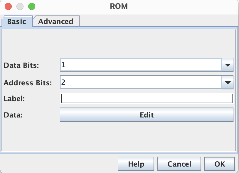
It will be your job to set the configuration:
log₂(8) = 3 address bits.Now, we want to copy and paste the DataValueForROM
column from control-signals.csv into the ROM. To edit the
contents of the ROM:
0b (e.g., 0b10000010) so that they are stored
correctly in the ROM.There are no automated tests for this task. You should manually check:
A to 0, the ROM outputs the microcode for
add.A to 1, the ROM outputs the microcode for
sub.In this task, you will complete your implementation of the control unit. Below you will find the interface of the control unit:
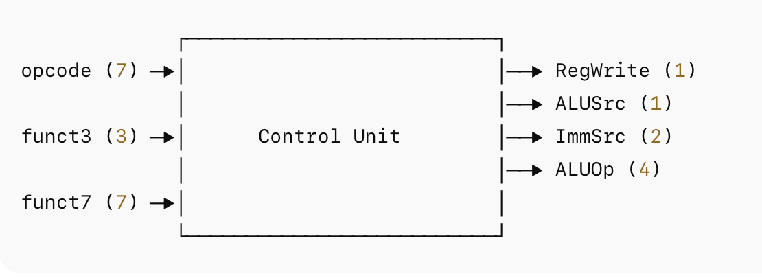
Your control unit will:
opcode,
funct3, and funct7 to determine which
instruction is being executed.is_add, is_sub,
is_and, …).RegWrite,
ALUSrc, ImmSrc, ALUOperation) as
control signals to the rest of the datapath.For reference, the RV32I encodings for the instructions we support are:
add : funct7 = 0000000,
funct3 = 000sub : funct7 = 0100000,
funct3 = 000and : funct7 = 0000000,
funct3 = 111or : funct7 = 0000000,
funct3 = 110slt : funct7 = 0000000,
funct3 = 010addi : funct3 = 000slti : funct3 = 010andi : funct3 = 111You can use comparators to match these bit patterns and produce one boolean signal per instruction.
Example for add:
opcode == 0110011funct3 == 000funct7 == 0000000is_add
signal.Do the same for each instruction (is_sub,
is_and, is_or, is_slt,
is_addi, is_slti, is_andi).
You will need to use a priority encoder to complete this task.
You can find the priority encoder at Components → Plexers → Priority Encoder.
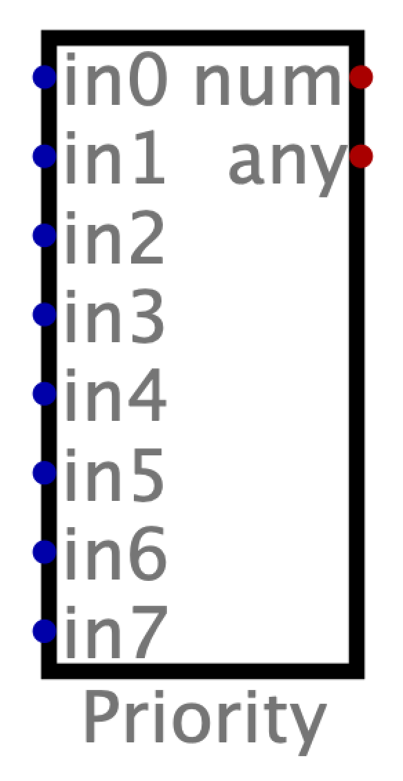
We will use an 8-input priority encoder where:
in0 … in7) corresponds to one
instruction (add, sub, and,
or, slt, addi, slti,
andi).num output is a 3-bit binary address
(0–7) that selects which instruction is active.any output is high whenever any of the
inputs are high.The priority encoder sets the num output to the binary
value of the highest-numbered input that is active (high). The highest
priority input is in7 and the lowest priority input is
in0. If multiple inputs are high (which should not happen
if your decode is correct), the encoder will choose the one with the
highest index.
The following truth table illustrates the operation of an 8-bit priority encoder:
| in0 | in1 | in2 | in3 | in4 | in5 | in6 | in7 | num | any |
|---|---|---|---|---|---|---|---|---|---|
| 0 | 0 | 0 | 0 | 0 | 0 | 0 | 0 | 0b000 | 0 |
| 1 | 0 | 0 | 0 | 0 | 0 | 0 | 0 | 0b000 | 1 |
| X | 1 | 0 | 0 | 0 | 0 | 0 | 0 | 0b001 | 1 |
| X | X | 1 | 0 | 0 | 0 | 0 | 0 | 0b010 | 1 |
| X | X | X | 1 | 0 | 0 | 0 | 0 | 0b011 | 1 |
| X | X | X | X | 1 | 0 | 0 | 0 | 0b100 | 1 |
| X | X | X | X | X | 1 | 0 | 0 | 0b101 | 1 |
| X | X | X | X | X | X | 1 | 0 | 0b110 | 1 |
| X | X | X | X | X | X | X | 1 | 0b111 | 1 |
is_add, is_sub, …, is_andi.in0..in7).num output is the ROM address
(A).D output is the 8-bit microcode for that
instruction.RegWrite, ALUSrc, ImmSrc,
ALUOperation) and send them to the datapath.An example test case for the add instruction is
below:
opcode   funct3  funct7    RegWrite ALUSrc ImmSrc1 ImmSrc0 ALUOp3 ALUOp2 ALUOp1 ALUOp0
0b0110011 0b000  0b0000000 0b1      0b0    0b0     0b0     0b0    0b0    0b1    0b0
It is your job to: - Add additional tests for the remaining instructions to verify that your control unit correctly decodes them and produces the right control outputs. —
The Instruction Memory and Program Counter have been set up for you
in cpu.dig.
The instruction memory is a ROM. We want the instruction memory to be able to store 1024 instructions, so the ROM should have 10 address bits. Each instruction is 32 bits, so the size of each entry in the instruction memory should be 32 bits. You can see the configuration of the ROM below.

In RV32I, the total addressable memory space is 4 GB or
232 bytes. The instruction memory for this lab is actually a
portion of the entire memory (specifically addresses
0x00003000 to 0x00003FFC). The size of our
instruction memory is 212 bytes (1024 instructions × 4 bytes
per instruction).
Our instruction memory component has 1024 entries, so we need to address it with log21024 = 10 bits instead of 32 bits.
Which bits of the program counter do we use to address the instruction memory?
There is nothing for you to complete for this task. Just make sure you understand the explanation above.
Complete cpu.dig by adding your:
alu.dig)register-file.dig)ALUSrc mux (to choose between rs2 and the
immediate)Important RISC-V details:
rd field of the instruction; there is no
RegDst signal in RISC-V.rs1 and
rs2.addi, slti,
andi), the ALU inputs are rs1 and the
sign-extended I-type immediate.rd (so RegWrite = 1 for all of them).ReadReg1 = rs1ReadReg2 = rs2WriteReg = rdRegWrite = control signal from your control unit /
ROMWriteData = ALU resultReadData1 (from register file)ALUSrc mux
ALUSrc = 0 → use ReadData2 (R-type)ALUSrc = 1 → use immediate (I-type)ALUOperation = control signal from your control unit /
ROMWhen you add the Register File, the input/output names may be
overlapping. To fix this, open your register-file.dig and
widen the component by clicking Edit → Circuit specific
settings and changing the width field.
To confirm that your circuit is functioning correctly, the provided
tests verify the values of ReadReg1 and
ReadReg2. To check these signals against expected values,
we have to make them outputs of cpu.dig. The output pins
have already been provided. Ensure you connect these output pins to
their corresponding signals.
Open basic-tests.s to view the RISC-V instructions used
to test your CPU. The program uses only:
add, sub, and,
or, sltaddi, slti, andiand sets up a few registers to known values so we can check your datapath.
We will use the miniRISC-V simulator/assembler.
basic-tests.s and take a look at the RISC-V
assembly instructions we’ve given you to start..mem file. Each line in this
file should contain one machine code instruction.The instructions need to be formatted to be compatible with Digital’s instruction memory.
Use format.py to convert the .mem file into
a .csv file containing a single 0b... 32-bit
binary word per line:
python format.py <input_file> <output_file>Replace .mem
file.
Replace .csv file.
For example
python format.py basic-tests.mem basic-tests.csv.csv file in Excel and copy the
contents.basic.txt into the
Digital testing unit.Once the basic tests pass, you will need to write additional tests
for the remaining instructions. Note, you will only pass as many tests
as you have instructions loaded up in memory. So if you just put the
first instruction in memory (addi x4, x0, -20), you will
only pass the first test.
Assignments are submitted through Gradescope.